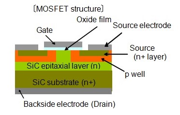
A typical or conventional SiC MOSFET uses the DMOSFET structure, here DD means double-diffused. As illustrated in the fig, the two source regions are arranged on the both side of the ground gate, while the drain is set on the backside. Furthermore, the DMOS structure consists of an n-type substrate on which is grown an n-epitaxial layer that forms the large drain region. The gate region is formed on the surface that overlies the graded p-type body implantation and diffusion area. The source regions are implanted and diffused on either side of the gate to form two separate transistors with a common drain region. The depletion regions will form around the source and p-body and these depletion regions can be connected by the field induced depletion region formed by the gate. The depletion region connecting the drain and source defines the channel and its dimensions are determined by the source and body doping.

In a result, the current flowing between drain and source terminals have both vertical and lateral components. Under a gate-induced channel which brings electrons near to the conduction band, electrons can be accelerated with a drain to source biasing. This basic MOS principle is also valid in DMOS devices. The two distinct transistor mentioned earlier may not have same characteristics, as the two source terminal matching is not perfect. This defect must be taken into account while designing circuits both in RF and power applications.
Firstly, silicon carbide devices can exhibit simultaneously high electro-thermal conductivity and extremely fast switching. This happens because SiC components are capable of handling high energy levels while operating at much higher switching frequencies. While, silicon carbide exhibits an operating temperature of at least 200°C, i.e. 50°C higher than the absolute maximum rating of silicon MOS devices, which allows SiC power devices to work well in a hot and hostile environment, enabling the appreciable gains in quality and reliability without performance de-rating.1
However, the high interface trap density reduces the utility of SiC. Additionally, compared with other novel design, the conventional design, DMOS is weak at broken isolation value, which may explain the price and market share of current SiC power devices.
Benefits and advantages of silicon carbide power devices over their silicon counterparts, Semiconductor Today ↩